
SiC-Coated Wafer Carriers for Planetary Epitaxy: Gas Foil Levitation Dynamics, Pocket Recess Tolerances, and Differential Warpage Control
Specify SiC-coated wafer carriers for planetary epitaxy: compare pocket tolerances, coating balance, and qualification evidence. Prepare a drawing-based RFQ.
SiC-coated wafer carriers for planetary epitaxy should be specified as a matched system: the finished pocket profile must suit the incoming wafer, the underside must suit the reactor's gas bearing, and the coating must retain acceptable geometry through the intended thermal cycle. No single pocket-depth tolerance or backside-flatness number establishes compatibility across reactor platforms.
For epitaxy process engineers, procurement teams, and supplier quality engineers, the practical purchasing question is which dimensions and evidence belong in the RFQ. This guide connects gas foil rotation, pocket recess, differential warpage, and handling interfaces to a drawing-based qualification plan. If you already have a controlled drawing, request a carrier feasibility review with the reactor configuration and wafer thickness range.
Published and technically reviewed: November 10, 2026. Scope: Global procurement of CVD SiC-coated graphite satellite carriers for planetary SiC CVD and GaN MOCVD configurations, with emphasis on 150 mm and 200 mm wafer handling. These processes have different chemistry and temperature requirements. Confirm the actual tool architecture before transferring any recommendation between them.
Evidence and limits: This is an engineering selection framework based on the public manufacturer and standards references below. It contains no Sicgraphite chamber trials, customer yield records, or measured carrier lifetime data. Numerical examples are explicitly hypothetical. Approved OEM drawings, licensed standards, fab recipes, and qualification results determine release limits.
Engineering and procurement takeaways
- Specify dimensions on the finished coated component and define the inspection datum, support condition, and temperature.
- Calculate wafer-to-rim step height from both pocket-depth and wafer-thickness distributions.
- Distinguish flatness, bow, warp, and rotational runout; they are different measurements.
- Qualify coating coverage, face-to-face balance, purity, and thermal-cycle stability together.
- Compare replacement sources using documented acceptance evidence and qualified cost per wafer pass.
1. Operating Mechanics: Planetary Reactors and Gas Foil Rotation
In a planetary arrangement, the main susceptor carries smaller satellite discs around the chamber while the satellites rotate about their own axes. This motion helps average exposure to the reactor's thermal and gas-flow fields. AIXTRON's G10-SiC product description identifies individual-wafer Gas Foil Rotation (GFR), automated loading, and configurations for nine 150 mm or six 200 mm wafers. Those statements establish platform context; they do not disclose replacement-part tolerances.
For a gas-supported satellite, the support flow produces a pressure field beneath the disc and supplies driving torque through the designed gas path. The support-gas circuit and the reactive flow above the wafer have different functions. Do not infer groove geometry, permissible gases, operating flow, or rotation speed from an illustration or a different reactor generation.
At steady lift, the integrated pressure difference across the supported area balances the weight of the carrier and its load. Rotation additionally requires sufficient driving torque to overcome drag. Underside deposits, gas-path restriction, changed carrier mass, or distorted geometry can disturb that balance. A rotation stall therefore requires a system diagnosis rather than an automatic conclusion that the carrier is out of flatness.
Thin-film lubrication models illustrate why gap geometry matters: for an ideal laminar, incompressible gap, pressure-driven conductance scales with the cube of gap height. Actual hot gas bearings may require compressibility, gas-property variation, and appropriate boundary conditions. This scaling is a sensitivity explanation, not a calculation of operating levitation height. Require the equipment owner's approved bearing-clearance and rotation checks instead of adopting a universal micrometer range.
2. Critical-to-Quality Pocket Recess and Wafer Fit
The pocket locates the wafer and influences its thermal contact and exposure to process flow. Its depth must be evaluated against the wafer thickness distribution, support geometry, coating buildup, and any intentionally designed floor contour.
Define the wafer-to-rim step before assigning a tolerance
For a flat wafer resting directly on the pocket floor, define recess as , where is finished pocket depth measured from the adjacent rim and is wafer thickness. Positive recess means the wafer top sits below the rim; negative recess means it protrudes. Bowed wafers, support lands, and shaped floors require additional local gap terms.
Hypothetical tolerance-stack example: Suppose an engineering drawing proposes a finished depth of and the incoming wafer specification is . Simple worst-case arithmetic gives a recess interval of to . A nominally flush design therefore does not guarantee flush wafers. These inputs are illustrative, not recommended SiC wafer dimensions or an approved carrier specification. Whether that interval is acceptable must be established for the specific process.
If the allowed recess interval is narrower than the combined variation, the available decisions include tighter finished-depth control, wafer thickness sorting, a different nominal depth, or a revised support profile. Each decision affects cost, handling, and thermal behavior. Record the selected tradeoff in the drawing revision so purchasing does not compare quotes built around different assumptions.
Flow and thermal consequences depend on the recipe
A wafer-to-rim step can perturb local flow and edge heat transfer. Its effect depends on pressure, velocity, chemistry, rotation, temperature, and the edge geometry. A particular step height does not universally trigger turbulence, wafer ejection, or a fixed percentage of thickness roll-off. Establish the useful recess window with process modeling or controlled qualification and measured wafer maps.
A center-high or edge-high floor changes where the wafer is supported and how the backside gap varies. The resulting thermal profile also depends on wafer bow, gas conduction, radiation, and the actual contact pattern. A deliberately contoured pocket may be appropriate for one recipe and inappropriate for another. See the related wafer slip and bow guide for the broader carrier–wafer thermal interface; use the approved process window to accept the component.
3. Engineering Cross-Section: Separate the Two Gaps
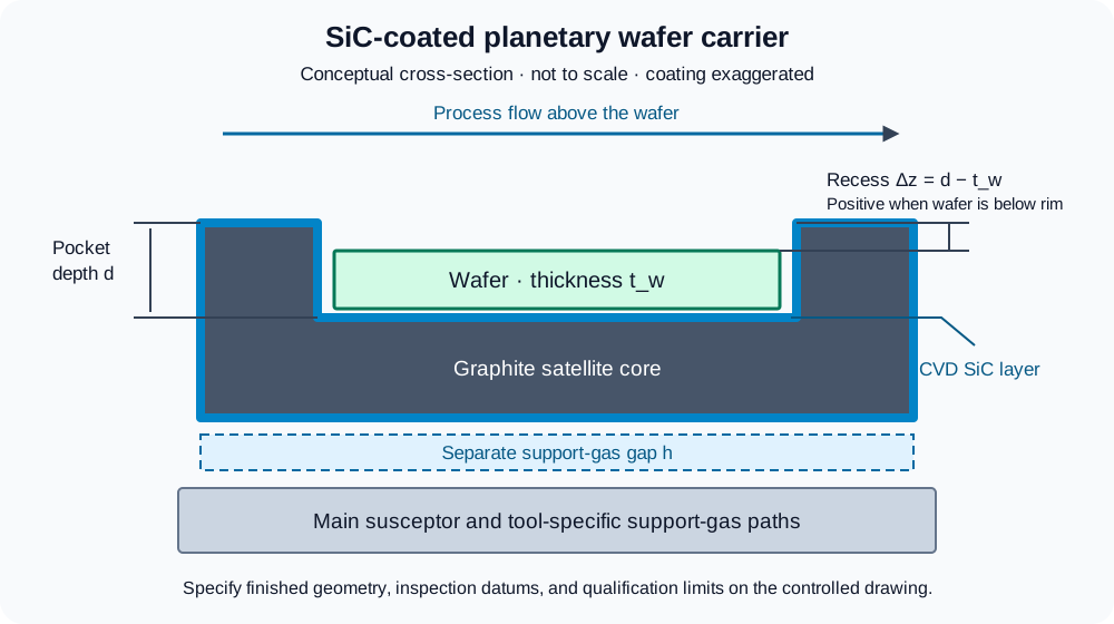
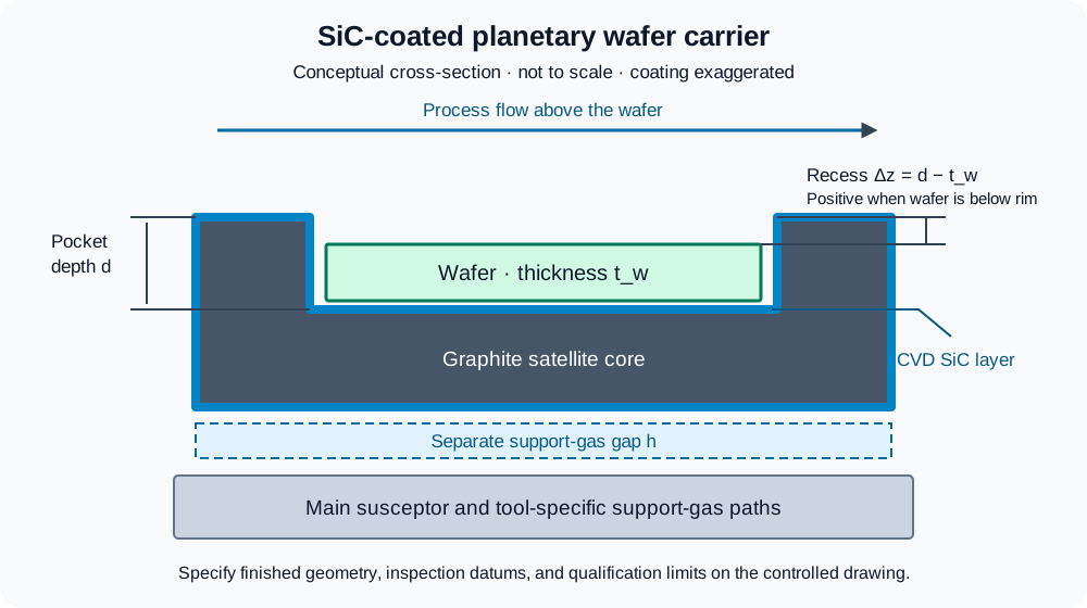
Figure 1. Original conceptual schematic, not to scale. The coating is exaggerated for visibility. Pocket depth, wafer-to-rim recess, and the underside support gap are separate dimensions. The drawing contains no OEM dimensions and is not evidence of manufactured-part performance.
Use this distinction when reviewing supplier inspection reports. A good pocket-depth result says nothing by itself about the underside bearing surface. Likewise, a flat underside does not demonstrate that every wafer pocket has the approved contour. Name both surfaces, identify their relationship to the inspection datum, and specify whether the component is measured freely supported or constrained in a fixture.
4. Differential CVD SiC Stress and Thermal Warpage
A thin coated carrier can change curvature because of residual deposition stress, differences in thermal expansion, temperature gradients, or asymmetric geometry. Matching graphite and coating expansion behavior is one part of the problem; it does not remove the need to measure finished shape and its stability.
Graphite properties vary by grade, direction, and temperature interval. Coating properties depend on deposition conditions and microstructure. Avoid treating a single handbook coefficient of thermal expansion as a full operating-temperature material specification. Ask for the proposed graphite grade, relevant property data, coating process controls, and evidence that the finished assembly meets its geometry requirements after the agreed thermal exposure.
Measure coating balance without turning it into a bow prediction
Hypothetical coating example: Top and bottom thicknesses of and differ by . If asymmetry is defined as absolute difference divided by mean thickness, the result is 20%. A supplier using a different denominator will report a different percentage, so the RFQ must define the calculation and sampling locations.
Those thicknesses alone cannot predict bow. A defensible stress model also needs elastic properties, residual stress, substrate thickness, pocket geometry, thermal history, and boundary conditions. For a shallow surface of approximately constant curvature , the geometric center-to-edge deflection scales as , where is the evaluated radius. This describes geometry after curvature is known; it does not supply the missing stress model.
Balanced deposition and suitable fixturing can reduce asymmetry, but simultaneous two-sided coating is not sufficient proof of stability and should not replace an acceptance result. Agree how representative coupons relate to the actual part, where thickness will be mapped, and what post-cycle changes in bow or warp are acceptable. Inspect edge coverage and pockets as well as broad faces.
Keep metrology terms distinct
Flatness describes a surface relative to two parallel enclosing planes. Bow and warp describe departures from a reference shape under a stated measurement convention. Total indicated runout measures indicator variation during rotation about a defined datum axis and includes alignment effects. An RFQ that calls all three “TIR” can produce incompatible reports. Define the measurand, datum, scan density, support, instrument capability, and acceptance decision rule before comparing suppliers.
5. Automated Handling, Thermal Clearance, and Optical Interfaces
Automated loading is a documented feature of the G10-SiC platform, but it does not establish a universal robot interface for every epitaxy tool. Relief scallops, lifting points, notch orientation, and transfer clearances must match the installed end effector and the permitted loading sequence. Check collision envelopes with the finished coating included. Edge radii and relief transitions also need coating-coverage and chip-risk review.
SEMI M55 addresses polished monocrystalline SiC substrate requirements. Its public abstract does not define carrier pocket depth or certify a robot interface. Put the applicable standard revision and agreed wafer dimensions in the purchase specification; obtain the licensed document where normative details are needed.
For thermal clearance, consider expansion of both members. The relevant quantity is the change in pocket diameter minus the change in wafer diameter. A wafer's absolute growth in diameter does not establish how much cold clearance is necessary when the carrier expands too. Allow for grade-specific expansion, unequal temperatures, wafer bow, coating geometry, and positioning uncertainty, then validate fit through the intended cycle.
Optical temperature readings depend on wavelength, emissivity, coating state, view factor, wafer transparency, and the instrument's correction method. Surface texture can influence the signal, but roughness alone cannot establish a fixed temperature error. Specify the surface finish and cleaning state required by the process, and correlate the reading against the approved calibration method. Do not prescribe mirror polishing to every pocket without checking its thermal and optical consequences.
6. Critical-to-Quality Specifications for the RFQ
The table below is a specification worksheet. All numerical limits must come from the controlled drawing and qualification plan; none of these rows supplies a universal OEM tolerance. State whether each dimension applies before coating, after coating, or after thermal conditioning. For a comparison of coating and substrate considerations, review CVD SiC-coated susceptors.
| Parameter | What the RFQ must define | Acceptance evidence | Risk being controlled |
|---|---|---|---|
| Carrier outer diameter | Finished envelope, datum, retaining clearance | Calibrated dimensional report | Interference and positioning error |
| Carrier thickness and mass | Finished thickness map and mass window | Dimensional and mass records | Bearing-load and thermal changes |
| Pocket depth | Nominal depth, tolerance, wafer thickness range | Pocket-by-pocket depth map | Uncontrolled wafer-to-rim step |
| Pocket floor profile | Flat or intentional contour; evaluation area | Surface profile with support condition | Changed wafer support and backside gap |
| Underside bearing surface | Flatness or approved profile; gas-path features | Full-area scan and dimensional checks | Gas leakage and contact drag |
| Coating coverage and balance | Thickness range, locations, asymmetry definition | Validated part or representative coupon measurements | Exposed graphite and stress imbalance |
| Rim radius and handling reliefs | Finished radii and end-effector envelope | Profile inspection and transfer trial | Chipping and robotic collision |
| Surface roughness | Measurement direction, cutoff, accessible areas | Traceable roughness report | Surface damage and process-interface variation |
| Purity and cleanliness | Element-specific limits, method, reporting limits | Lot-linked analysis and packaging record | Contamination and misleading certificates |
An instrument must be capable of resolving the requested tolerance. Ask how coating reflectivity, inaccessible pockets, probe force, and fixture restraint affect uncertainty. A dense point cloud with an unexplained best-fit plane can conceal the datum mismatch that matters during installation. Review the inspection method with engineering before making it a purchasing requirement.
7. Supplier Qualification: Compare Evidence and Total Cost
OEM and independent suppliers should be compared against the same acceptance package. Neither supplier category guarantees better purity, tighter inspection, shorter delivery, or lower total cost. Replacement compatibility depends on the exact component revision, chamber configuration, contractual permissions, and successful qualification. Use the SiC-coated wafer carrier product page to start a drawing review rather than treating a catalog listing as installation approval.
| Evaluation topic | Request from either source | Procurement decision |
|---|---|---|
| Part identity | Drawing revision, configuration, and deviation list | Reject unexplained substitutions |
| Graphite traceability | Grade, material lot, and relevant property data | Confirm the proposed material basis |
| Coating process | Coverage controls, thickness method, and repair policy | Check that controls address the actual geometry |
| Dimensional inspection | Agreed datums, uncertainty, and individual-part records | Compare equivalent acceptance evidence |
| Purity analysis | Sample location, lot identity, elements, and detection limits | Separate measured results from generic purity labels |
| Qualification support | Sample plan, process support, and failure response | Define who owns acceptance and corrective action |
| Delivery and cost | Dated quote, capacity assumptions, freight, and qualification costs | Compare achievable qualified supply |
Total cost per accepted wafer pass should include carrier purchase, qualification wafers, chamber time, cleaning, inspection, refurbishment, freight, and the number of accepted passes achieved. A cheaper unit may be more expensive if qualification or replacement frequency increases. Compare quotes using the same lifetime assumptions and show a sensitivity range until actual service data exist. This guide makes no percentage-savings or lead-time promise.
8. Sourcing and Quality Audit Checklist
Use the checklist with the inspection methods described on the quality and metrology page. Assign an engineering owner for each unresolved item before sample release.
- Confirm configuration: Record tool model, chamber revision, part identifier, wafer material and thickness distribution, and the authorized reference drawing.
- Freeze finished geometry: Identify critical datums, pocket contour, bearing surface, edge radii, coating allowances, and the inspection support condition.
- Review coating and material evidence: Link graphite and coating records to the part lot; agree thickness sampling, coverage checks, and permitted repair or recoating.
- Define purity acceptance: Specify elements and reporting limits. Bulk ash, a “5N” label, and element-specific GDMS results are different evidence and are not interchangeable.
- Control cleaning and packaging: Agree residue and particle requirements, compatible packaging materials, transport protection, and opening procedures with the receiving fab.
- Approve staged qualification: Begin with dimensional and transfer checks, then use the equipment owner's permitted rotation and thermal-cycle procedures. Define stop criteria and monitor wafer maps against an approved baseline.
- Control production changes: Set acceptance criteria for sample-to-batch transfer, periodic reinspection, refurbishment, and changes to material grade, machining, coating, or cleaning.
A fixed number of trial runs is not a substitute for this plan. The fab should choose the number and severity of exposures according to the process risk and available baseline data. Keep process qualification separate from incoming dimensional acceptance: a component can pass its drawing inspection while still requiring recipe-specific release.
9. Frequently Asked Questions
Why does a satellite carrier stop rotating after repeated use?
Possible causes include underside deposits, restricted support flow, changed bearing clearance, surface damage, or permanent distortion. Inspect the gas path and carrier against the equipment procedure and compare records with a known-good baseline. There is no service-life threshold established here, and cleaning or recoating should follow an approved method rather than an assumed cycle count.
Can pocket depth change when the wafer supplier changes thickness?
Yes, but first recompute the complete tolerance stack and review the support profile, thermal behavior, and handling envelope. A depth change requires drawing and qualification control. Machining an already coated pocket can expose graphite; ask whether the proposed change requires a new blank, recoating, or another approved manufacturing route.
Why use SiC coating rather than exposed graphite?
Toyo Tanso's public surface-treatment information describes dense CVD SiC as a way to protect the substrate and control particle and gas generation. Suitability still depends on coating integrity and the process environment. Do not assume absolute hermeticity, an unlimited chemical lifetime, or a guaranteed defect reduction from the coating name alone.
Does a low roughness value guarantee accurate pyrometry?
No. Roughness is one surface characteristic among several affecting optical response. Instrument wavelength, emissivity correction, wafer properties, and the viewed area also matter. Accept the finish together with the approved temperature-measurement procedure; a roughness certificate cannot establish an optical temperature-error limit by itself.
Are single-pocket and multi-pocket carriers interchangeable?
No. Pocket count changes the component envelope, load, thermal distribution, and handling arrangement. Confirm which disc and wafer layout the actual tool supports. Public batch wafer counts do not authorize a different satellite design or establish interchangeability between 150 mm and 200 mm configurations.
10. Sources and References
- AIXTRON — G10-SiC: Official platform description. Supports the stated wafer configurations, individual-wafer GFR, and automated loading context. It does not publish the pocket tolerances or gas-bearing clearances needed to approve a replacement.
- SEMI — M55, Specification for Polished Monocrystalline Silicon Carbide Wafers: Official standard catalog and abstract. Establishes the substrate standard's scope. The full normative document requires access; carrier geometry must be specified separately.
- Toyo Tanso — Surface Treatment, SiC Coating: Manufacturer technical information. Describes dense CVD SiC coating and particle/gas-control functions, with supplier-specific coating and impurity data. Those values are not Sicgraphite specifications or universal purchasing limits.
Public sources reviewed November 10, 2026. The tolerance-stack and coating-asymmetry examples are transparent engineering arithmetic, not reported experiments. Recheck this guide when the tool configuration, wafer specification, material grade, or coating route changes.
Request a drawing-based feasibility review
For a planetary carrier project, review our MOCVD and epitaxy solutions, then contact the engineering team with your drawing revision, reactor configuration, wafer specification, operating envelope, and required inspection evidence. Ask for a documented feasibility response, proposed deviations, and sample qualification plan before ordering production quantities. Manufacturing capability, acceptance limits, price, and delivery should be confirmed in the project quotation.
Author

More Posts
CVD SiC Coating vs. Bare Graphite in MOCVD: A Cost & Contamination Analysis
Why bare graphite fails in modern MOCVD. Analyze trace metal contamination, wafer slip, and the lifetime ROI of CVD SiC coated susceptors.
SiC Coated Graphite vs. Solid SiC Components: A Procurement & Engineering Guide
Compare SiC coated graphite vs. solid SiC for semiconductor components: purity, plasma resistance, machinability, lifespan, RFQ criteria, and tradeoffs.
C/C Composite Charging Trays and Grid Fixtures for High-Temperature Vacuum Furnaces: Creep Resistance, Eutectic Risk Mitigation, and Procurement Sizing
Specify C/C composite charging trays for vacuum furnaces: compare grid designs, assess contact-reaction risks, and prepare a drawing-based RFQ with Sicgraphite.