
RFQ Preparation Checklist
- Carrier/Susceptor drawings
- Target coating thickness
- Reactor type
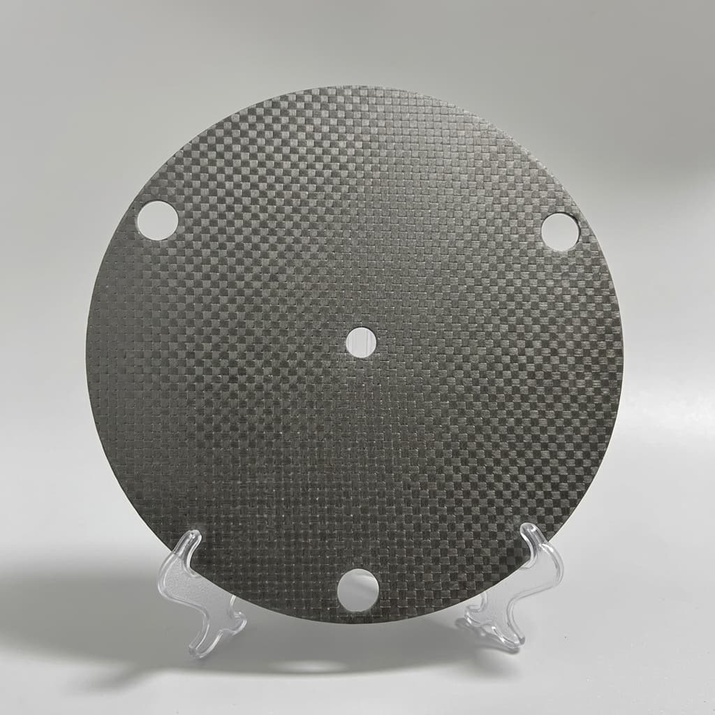
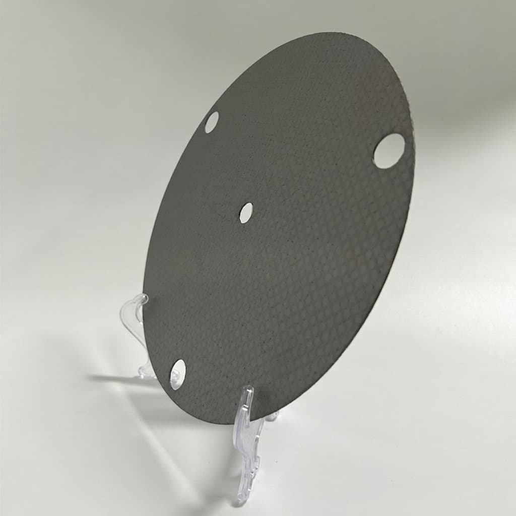
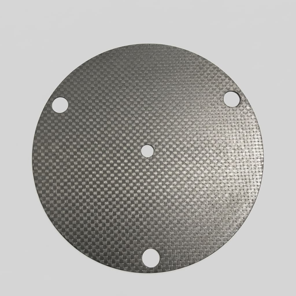
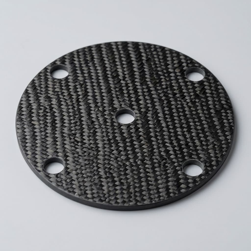
CVD SiC coated graphite components for MOCVD and epitaxial reactors. Preventing carbon dusting and resisting corrosive process gases like HCl and NH3.
| Evaluation Metric | Typical Range | Buyer Relevance |
|---|---|---|
| Coating Density | > 3.15 g/cm³ | Prevents gas permeation to graphite base. |
| Coating Uniformity | Thickness map or coupon check by project | Thin edges or pockets become the first failure point in corrosive epitaxy gases. |
| Base Graphite Match | CTE and density matched to CVD SiC coating | Poor substrate matching drives coating cracks, peeling, and exposed graphite. |
| Surface Finish | Ra target specified for wafer pocket or sealing surface | Surface finish affects wafer slip, particle risk, and thermal uniformity. |
| Decision Factor | Selection Logic | Buyer Check |
|---|---|---|
| Corrosive process gas | Choose CVD SiC coated graphite for MOCVD, epitaxy, HCl, NH3, or particle-sensitive wafer handling. | Specify gas environment, wafer size, equipment model, and lifetime target. |
| Coating feasibility | Deep pockets, blind holes, sharp edges, and hidden surfaces may need DFM changes before coating. | Ask for coating-thickness targets and note surfaces that must remain uncoated. |
| Substrate match | Base graphite must be chosen for CTE, density, and surface quality, not only machining cost. | Confirm CTE matching logic and first-article visual/coating inspection scope. |
| Stage | Delivery / QC Checkpoint | Buyer Evidence |
|---|---|---|
| 1. Coating DFM | Review pockets, blind areas, edges, masked surfaces, and coating-thickness target. | Marked drawing with coated, uncoated, and critical wafer-contact surfaces. |
| 2. Substrate machining | Machine graphite substrate with CTE, density, and surface preparation matched to CVD SiC. | Base material selection note and pre-coating inspection record. |
| 3. CVD SiC coating | Deposit dense SiC coating with attention to pockets, edges, and thermal-stress risk. | Coating thickness target and inspection method agreed before production. |
| 4. Final inspection | Check visible defects, coating continuity, dimensions, and wafer-contact surfaces. | Inspection report, photos, or coupon result depending on order scope. |
| 5. Clean export packing | Protect polished or coated surfaces from abrasion, fingerprints, and impact. | Individual wrapping, separators, and packing photos. |
Yes, we produce components that meet or exceed standard OEM specifications.
Early failure usually comes from substrate mismatch, coating shadow areas, sharp edges, or thermal cycling that creates cracks and exposes the graphite base.
No. Wafer-contact areas, gas-facing surfaces, edges, and masked interfaces should be marked on the drawing before the CVD coating route is finalized.
Ask for agreed coating-thickness checks, visual defect inspection, critical dimensional checks after coating, and clean packing photos for sensitive surfaces.
Inquiry Email
Include process, product type, drawing status, purity/coating target, dimensions, quantity forecast, operating conditions, and delivery date.
Instant Chat
+8618857971991
Best for quick drawing checks, process fit questions, and RFQ clarification.