
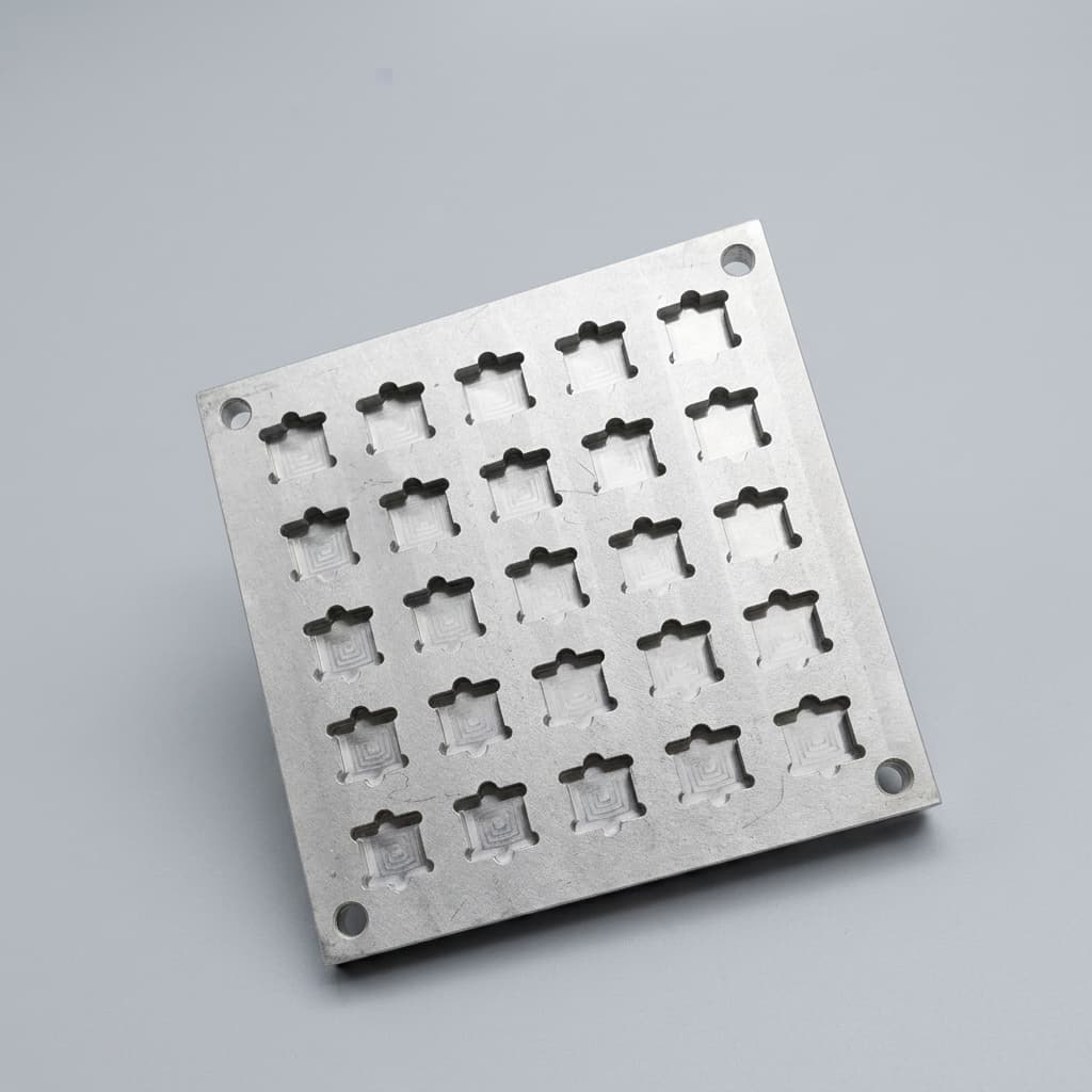
Preventing Wafer Slip and Bow in 200mm SiC Epitaxy: Susceptor Specifications
A comprehensive engineering and procurement guide to mitigating wafer slip, bow, and warp in 200mm SiC epitaxy through advanced SiC coated graphite susceptor design.
As the power electronics industry aggressively transitions from 150mm to 200mm Silicon Carbide (SiC) wafers to meet the surging demand for electric vehicles and renewable energy infrastructure, fab engineers and procurement teams are facing a brutal reality. The scale-up is not a simple linear progression. Processing 200mm SiC wafers at the extreme temperatures required for epitaxy (often exceeding 1600°C) amplifies thermal-mechanical vulnerabilities. Chief among these is wafer slip, an irreversible plastic deformation of the crystal lattice that destroys yield, alongside macroscopic defects like bow and warp.
For semiconductor equipment subassemblies, the susceptor—the component that physically supports and heats the wafer during the Chemical Vapor Deposition (CVD) epitaxial growth phase—is the single most critical variable in the thermal field. When dealing with 200mm substrates, standard 150mm susceptor designs fail catastrophically. The margin for error regarding thermal gradients, geometric flatness, and material emissivity has shrunk to near zero.
This comprehensive guide is designed for hardware engineers, process owners, and procurement specialists. It breaks down the thermomechanical mechanics of wafer slip, establishes the critical specifications required for SiC-coated graphite susceptors in 200mm processes, and provides an actionable framework for auditing suppliers and issuing RFQs.
Scope and limits (July 24, 2026): This guide applies to global RFQ, supplier-quality, and process-engineering reviews for 200mm 4H-SiC homoepitaxy reactors using CVD SiC-coated graphite susceptors. It is not a universal recipe for every MOCVD/CVD chamber, gas chemistry, wafer thickness, or carrier rotation profile. Treat the numeric ranges below as qualification targets to validate with your reactor thermal model, wafer bow metrology, coupon inspection, and tool-specific process window before production release.
The 200mm Economic Imperative
A single 200mm SiC wafer represents a massive financial investment. When a susceptor induces radial thermal gradients that trigger lattice slip, the wafer is often scrapped post-epitaxy. Upgrading to high-precision, CTE-matched, custom-profiled SiC coated graphite susceptors is not just an engineering preference—it is a mandatory yield-protection strategy that drastically lowers the Total Cost of Ownership (TCO).
1. The Physics of Wafer Slip, Bow, and Warp in SiC Epitaxy
Before specifying a susceptor, it is vital to understand the enemy. Silicon Carbide is an exceptionally hard and brittle material at room temperature. However, at the elevated temperatures required for high-quality homoepitaxial growth (1500°C to 1650°C), the crystal lattice becomes susceptible to plastic deformation.
What is Wafer Slip?
Slip occurs when localized thermal stresses within the wafer exceed the material's critical resolved shear stress (CRSS) along specific crystallographic planes (the basal planes in 4H-SiC). This stress forces the crystal planes to literally slide past one another. The result is a permanent dislocation network that propagates through the epi-layer, ruining the electrical characteristics of any device fabricated over that area. Devices built on slipped regions suffer from high leakage currents and premature breakdown.
The Role of Thermal Gradients
The primary driver of this excessive stress is temperature non-uniformity. When a 200mm wafer is heated, it expands. If the entire wafer is exactly the same temperature, it expands uniformly without internal stress. However, in reality, two types of thermal gradients plague the process:
- Radial Gradients (Center-to-Edge): If the center of the wafer is significantly hotter or cooler than the perimeter, the differing rates of thermal expansion create massive tensile and compressive stresses. Because the surface area of a 200mm wafer is nearly 78% larger than a 150mm wafer, managing radial gradients is exponentially more difficult.
- Axial Gradients (Bottom-to-Top): The bottom of the wafer is heated via conduction and radiation from the susceptor, while the top surface faces the cooler process gas inlet. This Delta T causes the wafer to bow (bend like a bowl).
How Bow Exacerbates Slip
When a wafer bows due to axial gradients, its physical contact with the flat susceptor pocket changes. The center may lift off the susceptor (loss of conductive heating), or the edges may curl upward, exposing them to different gas flows. This dynamic change in thermal contact instantly worsens the radial gradient, creating a vicious cycle that almost guarantees slip. Therefore, the susceptor must be engineered to either prevent bow or precisely accommodate the wafer's dynamic shape during the heating cycle.
2. Susceptor Architecture: The Core Material and Coating
A high-performance susceptor is a composite component. It consists of a meticulously selected isostatic graphite core enveloped by a high-purity, dense Chemical Vapor Deposition (CVD) Silicon Carbide coating. Both elements must operate in perfect harmony to manage the 200mm thermal field.
The Isostatic Graphite Core: Thermal Highway and CTE Matching
The graphite base is responsible for absorbing energy (often from an RF induction coil) and distributing it evenly to the wafer.
- Thermal Conductivity: Standard extruded graphite has anisotropic properties (it conducts heat differently depending on the direction). For 200mm epitaxy, premium ultrafine-grain isostatic graphite is non-negotiable. Isostatic graphite is pressed equally from all directions during manufacturing, resulting in isotropic thermal conductivity. This ensures that heat flows uniformly from the induction field to every millimeter of the 200mm pocket.
- CTE Matching: The Coefficient of Thermal Expansion (CTE) of the graphite must be precisely matched to both the SiC coating and, ideally, the SiC wafer itself. If the graphite expands faster than the coating at 1600°C, the coating will crack (delaminate). If the overall susceptor expands at a vastly different rate than the wafer, the wafer will scrub against the pocket edges, generating particulate contamination and stress points that initiate slip.
The CVD SiC Coating: Purity, Emissivity, and Protection
The CVD SiC coating serves three distinct purposes:
- Sealing the Core: It prevents the graphite from reacting with the highly aggressive hydrogen and silane/propane process gases, and stops carbon dust from contaminating the epi-layer.
- Thermal Transfer Interface: The surface roughness (Ra) and flatness of the SiC coating dictate how effectively heat transfers from the susceptor to the wafer. A coating that is too rough creates microscopic air gaps (thermal resistance). A high-quality coating must be uniformly thick (typically 50–150 µm) and incredibly smooth.
- Emissivity Control: The radiant heat transfer between the susceptor and the wafer depends heavily on the surface emissivity of the coating. Advanced susceptor manufacturers carefully control the morphology of the CVD SiC layer to stabilize emissivity, ensuring repeatable thermal profiles run after run.
Figure: Cross-section of a susceptor pocket demonstrating how wafer bow alters thermal contact, leading to radial temperature gradients and edge stress.
3. The Art of Susceptor Pocket Engineering
If the material properties form the foundation, the CNC machining of the susceptor pocket is the architecture that prevents slip. Because a 200mm wafer will inevitably bow slightly under extreme axial thermal gradients, the susceptor pocket cannot simply be a flat hole. It must be engineered to support the dynamic shape of the wafer.
Precision Profiling and Stepped Pockets
To combat center lift-off and edge curling, advanced susceptors utilize profiled pockets (often slightly concave or convex, mapped to micrometer tolerances) or stepped/terraced designs.
- A heavily engineered pocket ensures that even as the wafer bows, it maintains uniform thermal contact across its maximum possible area.
- By supporting the wafer slightly inward from the extreme edge, the pocket prevents the physical perimeter of the wafer from bearing the full mechanical load of the bow, eliminating a primary slip nucleation site.
Gas Flow and Saturation Trenches
The edges of the susceptor pocket often feature specialized geometries like localized gas trenches or angled bevels. These features manipulate the boundary layer of the process gas, ensuring that the concentration of precursors (Silane and Propane) is uniform across the massive 200mm span. If gas flow is disrupted by a poorly machined pocket lip, it induces localized cooling, re-introducing the thermal gradient that causes slip.
4. Structured Comparison: Susceptor Features vs. Yield Impact
When auditing a supplier's capability to deliver 200mm susceptors, procurement teams must look beyond the blueprint. The table below maps specific susceptor manufacturing characteristics directly to their impact on wafer slip and overall epitaxial yield.
| Susceptor Design / Manufacturing Feature | Impact on Thermal Field & Wafer Dynamics | Yield & Slip Prevention Outcome |
|---|---|---|
| Isostatic Graphite Core (Ultrafine Grain) | Ensures isotropic (uniform) 3D heat conduction from the RF field to the pocket. | Prevents localized hot/cold spots; drastically reduces radial thermal gradients that initiate basal plane slip. |
| Strict CTE Matching (Delta alpha below 0.5 x 10^-6/K) | Coating and core expand symmetrically. Wafer pocket dimensions remain stable during ramp-up. | Eliminates SiC coating micro-cracks; prevents wafer edge-scrubbing against pocket walls which causes mechanical stress. |
| Micrometer-Precision Profiled Pockets | Curvature matches the predicted dynamic thermal bow of a 200mm SiC wafer at 1600°C. | Maintains continuous thermal contact area; prevents center cooling and excessive edge-bearing loads. |
| Controlled Surface Roughness (Ra < 1.5µm) | Eliminates microscopic air gaps between the susceptor and the backside of the wafer. | Maximizes conductive heat transfer efficiency and consistency from run to run. |
| Optimized Edge Stepping / Gas Trenches | Smoothes the gas boundary layer flow over the critical perimeter of the massive 200mm surface. | Prevents edge-cooling effects caused by turbulent gas separation; ensures uniform epi thickness. |
| Uniform CVD SiC Coating Thickness | Ensures homogenous emissivity and identical thermal mass across the entire component. | Prevents asymmetrical radiant heating, keeping the overall Delta T across the 200mm span strictly within safe tolerances. |
5. The Procurement and Engineering Checklist
Sourcing a 200mm susceptor is a complex technical procurement exercise. Relying on legacy 150mm prints with scaled-up dimensions will inevitably lead to yield crashes. Use this checklist when qualifying a new vendor or issuing an RFQ for 200mm SiC epitaxy components:
- Graphite Grade Verification: Has the supplier specified the exact grade of isostatic graphite? Request data sheets proving grain size (below 10 µm preferred) and isotropic thermal conductivity.
- CTE Data: Demand documented proof of the CTE match between the chosen graphite core and their proprietary CVD SiC coating across the 1000°C–1600°C range.
- CNC Machining Tolerances: Can the supplier reliably machine complex, non-flat (concave/convex) pocket profiles to single-digit micrometer tolerances? Ask for CMM (Coordinate Measuring Machine) reports of sample pockets.
- Coating Uniformity Maps: Do not accept bulk average thickness. Request a thickness distribution map for the CVD SiC coating, especially inside the intricate corners of the wafer pocket.
- Purification Route: For 200mm wafers targeting high-voltage power devices, deep halogen purification of the graphite core prior to coating is mandatory. Confirm the supplier runs high-temperature halogen purification.
- Metrology and QA: How does the supplier measure the surface roughness and flatness of the SiC coating post-deposition? Ensure their metrology tools can handle 200mm+ diameter spans without relying on localized spot checks.
6. Frequently Asked Questions (FAQ)
Q: Why can't we just use a thicker 200mm wafer to resist thermal bow and slip?
A: While increasing substrate thickness increases mechanical rigidity, SiC material is astronomically expensive. The industry mandate is to reduce substrate thickness to lower costs. The burden of maintaining flatness and preventing slip falls entirely on the thermal management of the reactor and the susceptor.
Q: Does the rotation speed of the planetary susceptor affect thermal gradients?
A: Yes. Planetary rotation averages out macro-level thermal non-uniformities in the chamber. However, rotation cannot fix a badly designed pocket. If the pocket allows the wafer to bow and lose contact, the wafer will slip regardless of how fast it spins.
Q: How often should a 200mm SiC coated graphite susceptor be replaced?
A: Susceptors are consumables. In high-volume 200mm epi, the SiC coating degrades from plasma cleans (HCl) and thermal cycling. Once the coating roughness changes significantly, emissivity and thermal contact drift, leading to a sudden spike in wafer slip. PM (Preventative Maintenance) cycles vary, but typically range from 50 to 200 runs depending on the aggressiveness of the chemistry and the quality of the initial component.
Q: Can we coat the susceptor with Tantalum Carbide (TaC) instead of SiC for 200mm epitaxy?
A: TaC coatings are extremely stable at high temperatures and resist hydrogen etching better than SiC, extending lifespan. However, TaC has a different emissivity profile and cost structure. If you are exploring this, read our dedicated comparison on TaC vs. SiC Coating in PVT/Epitaxy.
Q: If a wafer slips, does it damage the susceptor?
A: Not directly. However, the conditions that caused the slip (e.g., a localized hot spot or degraded coating) will remain and destroy the next wafer. Furthermore, if a heavily bowed wafer causes mechanical friction or chips against the pocket edge, it can generate particles that compromise the susceptor's pristine surface.
7. Conclusion
Mastering the 200mm SiC epitaxy transition requires recognizing that the susceptor is no longer just a holder—it is an active, highly engineered thermal management device. Wafer slip is the ultimate penalty for failing to control thermal gradients. By specifying premium isostatic graphite, mandating strict CTE matching, demanding micrometer-level pocket profiling, and enforcing rigorous coating uniformity standards, fabs can eliminate slip, conquer bow, and realize the massive economic advantages of the 200mm era.
Ready to Scale to 200mm Without Compromising Yield?
Do not let poorly engineered susceptors bottleneck your 200mm SiC production. At SiC Graphite, our engineering team collaborates directly with process owners to design and manufacture custom-profiled, ultra-high-purity SiC coated graphite susceptors optimized for extreme thermal uniformity. Contact our technical sales engineers today to discuss your pocket geometry, request CTE validation data, and secure your supply chain.
8. Sources and References
- Journal of Applied Physics (AIP): Analysis of basal plane dislocation formation in 4H-SiC wafers under stress, including wafer-edge BPD half-loop formation and the relationship between wafer warp, radial temperature gradients, and thermal stress during post-growth annealing. https://pubs.aip.org/aip/jap/article/135/23/235706/3298663/Formation-of-basal-plane-dislocations-by-stress
- SGL Carbon: SIGRAFINE® SiC coating overview, detailing CTE matching principles between isostatic graphite and CVD SiC, and its critical role in preventing thermal stress and delamination in semiconductor applications. https://www.sglcarbon.com/en/markets-solutions/material/sigrafine-sic-coating/
- CoorsTek: Technical data on PureSiC® CVD Silicon Carbide and high-purity graphite, emphasizing the necessity of isotropic thermal conductivity and ultra-high purity for advanced 200mm wafer processing. https://www.coorstek.com/en/materials/silicon-carbide/
- Mersen: Advanced material specifications for purified graphite and silicon carbide composites, highlighting the impact of precision CNC machining and tailored coating thickness on semiconductor yield and thermal management. https://us.mersen.com/sites/default/files/files_imported/2-gs-purified-graphite-silicon-carbide-graphite-mersen.pdf
Author

More Posts
SiC Coated Graphite vs. Solid SiC Components: A Procurement & Engineering Guide
Compare SiC coated graphite vs. solid SiC for semiconductor components: purity, plasma resistance, machinability, lifespan, RFQ criteria, and tradeoffs.
How to Choose High-Purity Isostatic Graphite for Semiconductor Crystal Growth
A buyer's guide to isostatic graphite for SiC PVT and silicon CZ growth. Learn how grain size, bulk density, and ash content affect yield.
CVD SiC Coating vs. Bare Graphite in MOCVD: A Cost & Contamination Analysis
Why bare graphite fails in modern MOCVD. Analyze trace metal contamination, wafer slip, and the lifetime ROI of CVD SiC coated susceptors.